EMPOWER YOUR DESIGNS BACKED BY INDUSTRY-TESTED MULTIPHYSICS ANALYSIS
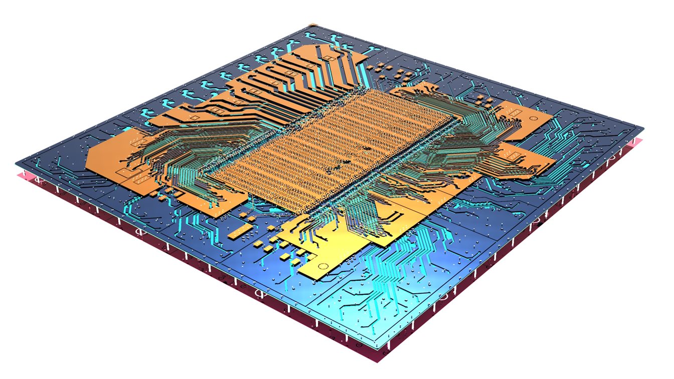
The semiconductor industry is currently experiencing a transformative phase, driven by advancements in manufacturing technologies. This transformation is characterized by two significant challenges confronting semiconductor designers. Firstly, the relentless progression of Moore’s Law has led to the adoption of cutting-edge finFET process technologies, pushing transistor architectures to increasingly smaller dimensions below 5nm. This evolution includes innovative transistor designs such as nanosheet gate-all-around (GAA) and novel approaches to power delivery, such as back-side power delivery. Secondly, designers are grappling with the complexities of multi-die design, 2.5D/3D-IC packaging, and heterogeneous integration. Leading design teams are embracing these advancements to tackle the intricacies of 3D-ICs, encountering a myriad of novel multiphysics challenges in the process. These challenges span various domains, including electrical, thermal, and mechanical considerations, as designers strive to achieve success in this new era of semiconductor design.
Capabilities
IR-Drop Signoff
Ansys RedHawk-SC ensures the integrity of power delivery networks by verifying and mitigating voltage drop issues, thereby preventing potential failures due to inadequate power distribution.
Static and Dynamic Power Integrity Analysis
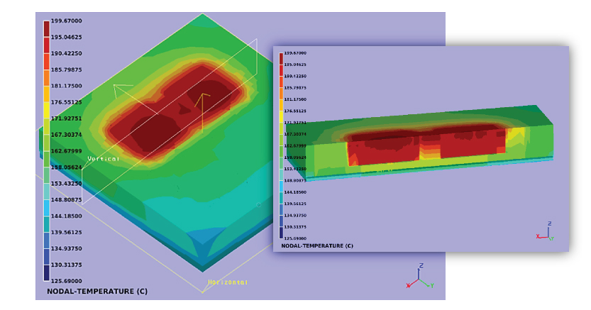
The entire power distribution network of the 2.5D/3D package undergoes analysis for IR-drop, current density, and electromigration. Individual pad peak currents are reported, with all analyses being thermal-aware, accounting for Joule self-heating.
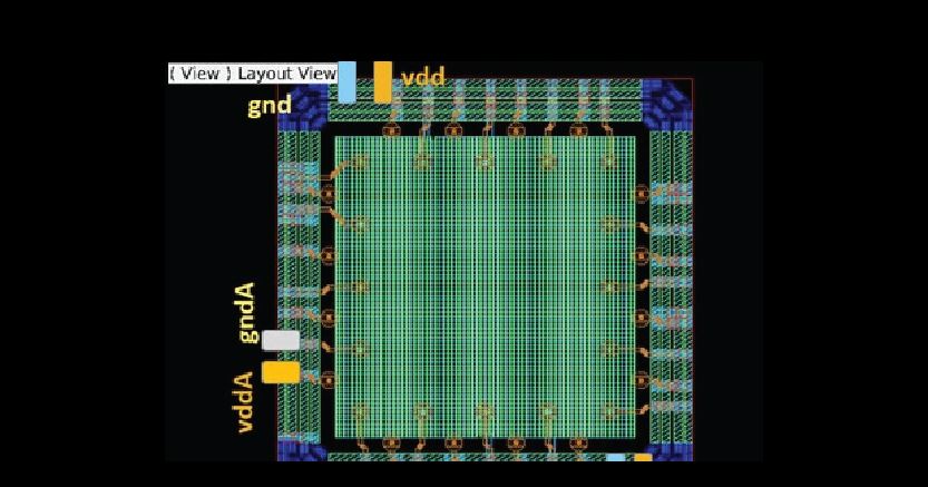
Power Integrity and Noise Verification at Transistor Level
Meticulously analyze power distribution at the transistor level to mitigate noise issues and optimize design integrity, ensuring robust performance.
ESD Integrity Simulation
Ansys PathFinder-SC provides advanced ESD integrity simulation by replicating HBM and CDM events to identify and resolve layout bottlenecks. It models current injection into pads and pathways, detecting vulnerable pin-clamp-pin paths to ensure robust ESD protection and design reliability.
Integration Extraction and Simulation Engineer
Ansys PathFinder integrates extraction and simulation engines to analyze current density and reliability in semiconductor designs comprehensively. This seamless integration facilitates optimized layout and enhanced performance insights.
Foundry Certified Silicon Correlation
Ansys PathFinder offers foundry-certified silicon correlation, ensuring accurate alignment between simulation results and actual silicon performance in semiconductor designs. This capability provides confidence in design accuracy and reliability during the manufacturing process.
Capacity to Analysis Full SOC's
Ansys PathFinder-SC provides comprehensive analysis, planning, verification, and sign-off for full SoC designs, ensuring integrity and ESD robustness.
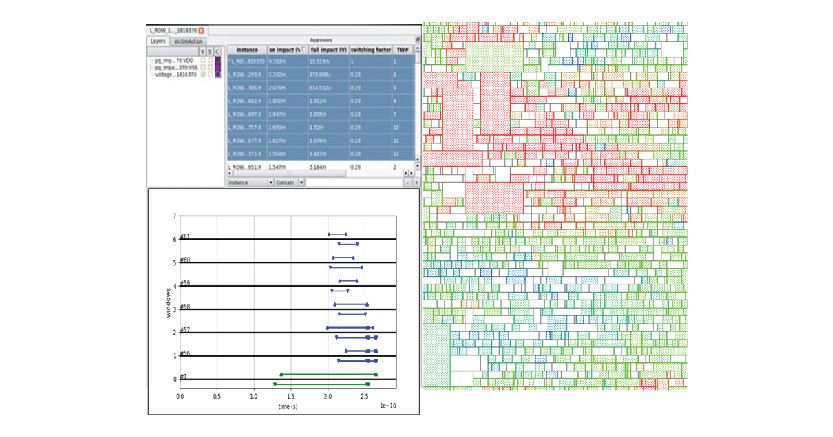
RedHawk-SC is the premier solution for power noise and reliability signoff, renowned for its reliability in digital IP and SoCs scaling down to 3nm. It boasts a cloud-native elastic compute infrastructure, ensuring scalability and flexibility to meet the evolving demands of semiconductor design. As the trusted industry leader, RedHawk-SC provides comprehensive support for power integrity verification, enabling designers to achieve optimal performance and reliability in their designs while leveraging cutting-edge technology and cloud resources.
Ansys RedHawk-SC Electrothermal offers unparalleled solutions for intricate electrical and thermal multiphysics challenges in multi-die 2.5D/3DIC structures. Leveraging top-tier engines from Ansys RedHawk-SC, it precisely tackles power, signal integrity, and mechanical stress equations within heterogeneous systems. This platform ensures accuracy by solving electrothermal and mechanical equations while utilizing the elastic compute infrastructure for high-throughput analysis of up to a billion instances concurrently. Additionally, it provides comprehensive prototyping capabilities with early block power estimates and seamless integration with thermal analysis tools like AEDT/Icepak for boundary conditions from system-level analyses.
Ansys Totem™ revolutionizes transistor-level power integrity and reliability analysis, empowering users to conduct thorough assessments on analog mixed-signal IP and full-custom designs. It reshapes the conventional flow of analog mixed-signal power noise and reliability analysis by accommodating various design environments for modeling and characterization. Totem boasts a robust extraction and simulation engine, complemented by an intuitive graphical interface for in-depth root cause analysis and debugging of results.
Power Integrity and Noise Verification at Transistor Level
Totem-SC offer an ultra high-capacity version of Totem
Capacity for several million xtor flat
Simultaneousl simulation of digital and analog blocks
Ansys PathFinder-SC detects and isolates the root causes of design issues that may result in chip failure due to charged-device model (CDM), human body model (HBM), or other ESD events. Its high-capacity, cloud-native architecture leverages thousands of compute cores for fast full-chip analysis. PathFinder-SC is certified by major foundries for resistance and current density checks required for ESD signoff.
Ansys PathFinder-SC is a high-capacity solution designed for comprehensive analysis of full SoC designs. It facilitates detailed planning, verification, and sign-off processes to ensure design integrity and robustness against electrostatic discharge (ESD).
Ansys PathFinder's integrated extraction and simulation capabilities optimize semiconductor layout and performance by analyzing current density, ensuring reliability and efficiency in electronic systems.
View Application
Design Enhancement
Ansys PathFinder enhances semiconductor reliability and performance by analyzing current density at layout and netlist levels, optimizing design for efficient power distribution and preventing overheating risks. Through comprehensive dual-level assessment, it ensures robustness and longevity in electronic systems.
View Application
Current Management
Ansys PathFinder analyzes current density in semiconductor designs to ensure even distribution, mitigating overheating risks and potential failures. By identifying high-current areas and optimizing layout, it enhances design reliability and performance.
View Application
ESD Integrity
Ansys PathFinder-SC's ESD integrity simulation ensures the robust protection of semiconductor designs against Human Body Model (HBM) and Charged Device Model (CDM) events, ultimately enhancing the reliability of electronic devices.